English
Alpha-Ta Films Explained: Phase Control, Purity, and Sputtering Targets
Content
Alpha-tantalum, written α-Ta in papers and fab specifications, is the body-centred cubic phase of tantalum, and it is the phase that superconducting quantum circuits and advanced semiconductor stacks actually want. Sputter tantalum onto a room-temperature silicon wafer with its native oxide still in place and you usually get beta phase instead: roughly nine times the resistivity, a superconducting transition temperature below 1 K, and an oxide interface that quietly caps coherence.
The short version: alpha phase is a result you engineer, not a grade you order. Substrate temperature, seed layer, working pressure and film thickness decide which phase grows; the oxygen content, purity and grain structure of the tantalum you start with decide how wide that process window is. When incoming metal carries too much oxygen or interstitial nitrogen, parameter tuning stops working, and you discover it on the coherence data or the particle count after the wafers are already processed.
Representative mid-range values from the literature for sputtered tantalum films; actual values shift with deposition conditions and impurity content. Each panel is drawn to its own scale.
That gap between the two bars is the reason phase control is treated as a process problem rather than a materials footnote. What follows is what α-Ta is, how it forms in a sputter tool, where the supply chain can break it, and which specification fields are worth arguing about before you sign a purchase order.
What Alpha-Ta Is, and Where Beta-Ta Comes From
Tantalum has two thin-film personalities and they behave nothing alike. Alpha-tantalum is the bulk-stable body-centred cubic phase. Beta-tantalum is a metastable tetragonal phase that forms readily when arriving atoms land on a cold, amorphous or oxidised surface and lack the energy to arrange themselves into the BCC lattice. On a room-temperature wafer carrying a nanometre or two of native SiO2, beta is the default outcome. A heated substrate or a crystalline seed layer tips the balance the other way.
Both phases are genuine tantalum. The difference is structural, and it shows up in every electrical number that matters downstream.
| Property | α-Ta (BCC) | β-Ta (tetragonal) |
|---|---|---|
| Crystal structure | Body-centred cubic, bulk-stable | Metastable tetragonal (β-U type) |
| Room-temperature resistivity | Approximately 15 to 25 µΩ·cm | Approximately 150 to 200 µΩ·cm |
| Superconducting transition temperature | Near 4.4 K | Roughly 0.5 to 0.9 K |
| Typical as-deposited condition | Heated substrate or Nb / TaN seed layer | Room temperature on native oxide |
| Common device uses | Qubit metal, low-loss resonators, copper diffusion barrier | Thin-film resistors, some barrier stacks |
| Behaviour on anneal | Stable to high temperature | Shifts towards alpha at elevated temperature |
How α-Ta Films Form During Sputtering
Almost all α-Ta used in devices today is deposited by magnetron sputtering, whether DC, RF or HiPIMS, from tantalum targets in the 4N to 5N range. Recent growth studies comparing sapphire, silicon and photoresist lift-off substrates keep reaching the same conclusion: the film does not choose its own phase, the process chooses it.
Four levers that decide the phase
- Substrate temperature. Above roughly 400 °C on silicon, adatoms gain enough surface mobility to settle into the BCC lattice; below that, the tetragonal phase nucleates first and often stays.
- Seed layers. A thin Nb, TaN or TiN layer offers a template with a closer lattice match to α-Ta than amorphous SiO2 does, and it also blocks oxygen diffusion from the substrate.
- Working pressure and ion energy. Lower pressure with moderate energetic ion bombardment densifies the growing film and favours alpha nucleation, while very high pressure tends to give porous columnar beta.
- Thickness and rate. Phase content can drift with thickness, so a stack that nucleates in alpha may not remain there through a 200 nm layer if the deposition rate is pushed too hard.
Why the feedstock still matters
Each of those levers is really a fight against oxygen and nitrogen. Interstitial impurities raise the energy barrier for the BCC phase and stabilise beta, which is precisely why targets with tighter oxygen and nitrogen limits tolerate wider process windows and give you more room to tune temperature and pressure.
If your stack uses a niobium seed layer, the most common template for alpha growth, the seed metal needs the same purity discipline as the tantalum above it, because a contaminated seed simply moves the problem one interface further down.
 Niobium ingotPurity: 99.99% Maximum Dimensions: 400mm Maximum Weight: 2 tons Packaging: Wrapped in stretch film. Outer boxes are packed in export-friendly wooden crates with pearl ...View Product →
Why Quantum and Semiconductor Teams Specify the Alpha Phase
In a superconducting qubit, every source of loss shows up as a shorter coherence time. Phase is not a cosmetic detail, it changes four things at once:
- Microwave loss. Resistivity in the 15 to 25 µΩ·cm range keeps resonator and interconnect losses low, which simplifies circuit design.
- Operating margin. A transition temperature near 4.4 K keeps devices comfortably superconducting at dilution-fridge temperatures, with headroom for local heating.
- Interface quality. Alpha films grown on sapphire or on a proper seed layer produce sharper metal-to-substrate interfaces and fewer two-level system defects, the dominant decoherence mechanism in planar transmons.
- Barrier behaviour. Where tantalum acts as a copper diffusion barrier in interconnect stacks, a dense BCC film outperforms a porous tetragonal one.
The payoff is measurable. Work published in 2021 showed tantalum-based transmon qubits on sapphire exceeding 0.3 milliseconds of coherence, several times what comparable niobium and aluminium devices delivered. That result only reproduces when the film is alpha phase, low in oxygen and consistent from wafer to wafer.
From Ingot to Target: The Purity Chain Behind Alpha-Ta
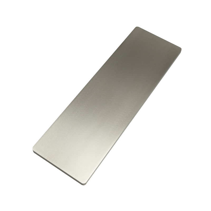
Device-grade α-Ta begins long before the sputter chamber. The industrial chain runs from purification and melting through casting, then to rolling, forging or machining into the target geometry the tool requires. Each step either adds or removes the oxygen and metallic contamination that later defines your phase window.
Schematic: the four stages of the tantalum supply chain in processing order (1 to 4). Segments are equal in size for illustration only and do not represent share of cost, time or contamination risk.
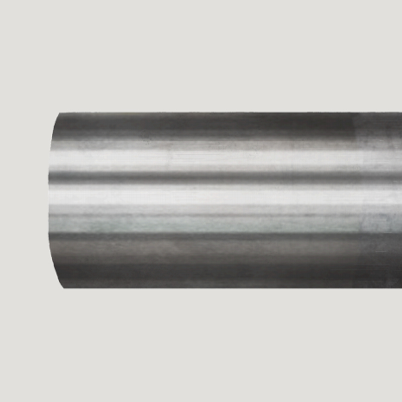
Two numbers in that chain deserve attention. The first is purity: 4N (99.99%) tantalum is common, 5N (99.999%) is specified for the most loss-sensitive work, and what usually matters is not the headline figure but the individual limits on sodium, potassium, iron, copper, tungsten and molybdenum, magnetic and mobile species that degrade coherence even at ppm levels. A tantalum ingot produced by vacuum melting gives a cleaner starting point than a re-melted scrap route, and that difference survives all the way into the film.
The second number is oxygen. Electronic-grade tantalum is generally held well under 100 ppm, and the analytical report should come from GDMS for trace metals plus inert-gas fusion for oxygen, nitrogen and hydrogen. Grain structure and density matter just as much on the target side: a dense target with fine, uniform grains sputters at a stable rate and throws fewer particles, while a porous or coarse-grained one drifts and forms nodules that end up as film defects.
 high purity ta metals supplierTantalum ingot Purity: 99.99% Maximum Size: Customizable Maximum Weight: Customizable Packaging: Wrapped in stretch film. Outer boxes are packed in export-friendly woo...View Product →
Purchase Specs Worth Writing Into the PO
Most phase problems that reach a fab trace back to a purchase order that described the metal too loosely. These are the fields worth stating explicitly rather than leaving to "standard commercial quality".
| Specification | Practical target | Why it matters |
|---|---|---|
| Bulk purity | 4N5 to 5N, certified per lot | Sets the baseline for trace metal control |
| Oxygen | Below 100 ppm, below 50 ppm for loss-critical films | Oxygen stabilises beta phase and raises interface loss |
| Magnetic traces (Fe, Ni, Cu) | Agreed ppm ceilings, reported by GDMS | Even ppm levels shorten qubit coherence |
| Alkali metals (Na, K) | Single-digit ppm | Mobile ions drift under bias in oxide stacks |
| Density | 99% of theoretical or higher | Low porosity means fewer particles and stable rate |
| Bonding | Void-free, verified by C-scan | Voids cause hot spots, arcing and early target failure |
| Traceability | Lot-level records under ISO 9001 and IATF 16949 | Makes a phase excursion traceable back to material |
Ask for tolerances on thickness, flatness and grain size as well. A target that meets a purity claim but misses dimensional tolerance will still cost you a sputter campaign, and for semiconductor applications, requalification is far more expensive than the metal itself.
FAQ
Can I get alpha-Ta on a room-temperature wafer?
Yes, with help. A thin Nb or TaN seed layer allows α-Ta to nucleate at or near room temperature because the template removes the need for high adatom mobility. Without a seed layer, room-temperature deposition on oxidised silicon normally gives beta phase.
Is 5N tantalum always better than 4N?
Not automatically. Two 5N lots with different oxygen and iron levels can behave very differently in the same sputter tool. Compare the full analytical certificate rather than the number of nines on the label.
How do I confirm which phase I actually got?
X-ray diffraction is the direct answer: α-Ta shows the BCC (110) reflection near 38.5 degrees, while β-Ta is identified by its (002) peak near 33.6 degrees. Sheet resistance and residual resistance ratio are fast proxies, since alpha films sit at low resistivity and beta films at several times that value.
Alpha-Ta is a phase-control problem that starts with the metal, not with the recipe. Get the oxygen and trace metal profile right, keep density and grain structure under control, and the process window stays wide enough to work with. CRNMC produces ultra-high-purity tantalum and related metals through purification, melting, casting and processing, across five production bases and eight material families, under ISO 9001 and IATF 16949, and offers purity testing alongside standard order support. Send the specification your film stack is working to, and we will tell you what is achievable from the feedstock side.