English
What Makes Titanium Targets the Critical Enabler of Next-Generation Thin-Film Manufacturing?
Content
- 1 Market Size and Growth Drivers: Downstream Applications Fuel Demand Expansion
- 2 Technical Barrier Analysis: Purity, Density, and Grain Control
- 3 Competitive Landscape: Domestic Substitution Accelerates, but Gaps Remain in the High-End Market
- 4 Application Frontiers: Emerging Demand from Medical Devices and Aerospace
- 5 Supply Chain Investment and Procurement Decision Recommendations
Titanium targets, as the core consumable in physical vapor deposition (PVD) processes, have market demand tightly coupled to the development of high-end manufacturing sectors including semiconductors, flat-panel displays, photovoltaics, and medical devices. The industry currently exhibits three definitive trends: first, the global market is expanding at a compound annual growth rate (CAGR) of 8.5% to 10.2%; second, the domestic substitution of ultra-high-purity (5N and above) targets is accelerating; and third, large-size, high-uniformity targets have become the primary field of technological competition. For industry chain participants, mastering high-purity titanium raw material purification and precision forming technology is fundamental to gaining market initiative over the next five years.
Market Size and Growth Drivers: Downstream Applications Fuel Demand Expansion
The market size of titanium targets does not exist in isolation; it is directly determined by capital expenditure in downstream application sectors. According to data from industry research institutions, the overall global sputtering target market was approximately USD 4.5 billion in 2024, with titanium targets accounting for about 12% to 15%, corresponding to a market size of roughly USD 540 million to 680 million. This figure is projected to exceed USD 1.1 billion by 2030.
Semiconductor Sector: The Most Stringent and Fastest-Growing Market
In the metal interconnect and barrier layer deposition processes of logic and memory chips, titanium targets are irreplaceable materials. As advanced processes push toward 3nm and below, purity requirements for targets have risen from conventional 4N (99.99%) to 5N5 (99.9995%) or even 6N (99.9999%). A single 12-inch wafer fab can consume 3,000 to 5,000 pieces of targets annually (converted to standard sizes), and the unit price of high-end targets is 3 to 5 times that of standard display targets.
Flat-Panel Display and Photovoltaics: Large-Size Trends Drive Target Specification Upgrades
TFT-LCD and OLED panel production lines continue to evolve toward Gen 10.5/11, with target sizes expanding from early diameters of 200mm to over 400mm in diameter and lengths exceeding 3,000mm. In the heterojunction (HJT) solar cell sector, the application of titanium-based transparent conductive films has driven photovoltaic target demand to achieve a CAGR of over 25% between 2020 and 2024.

Technical Barrier Analysis: Purity, Density, and Grain Control
Titanium targets are not simple metal fabricated parts; their performance directly determines the quality of sputtered thin films. Industry technical barriers concentrate on the following three dimensions:
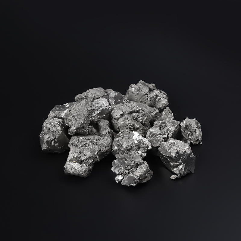
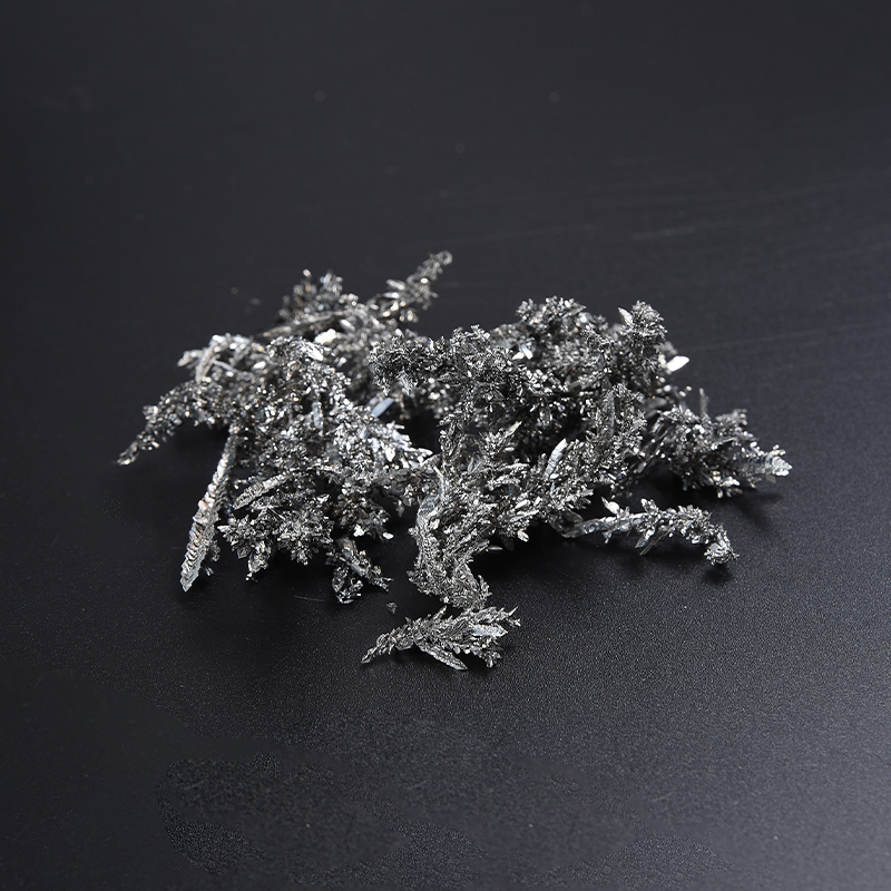
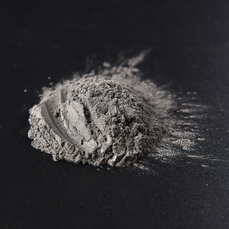
1. Raw Material Purification: The Leap from Sponge Titanium to High-Purity Titanium
Industrial-grade sponge titanium typically has a purity of 2N to 3N, while target-grade high-purity titanium requires multiple rounds of purification through electron beam cold hearth remelting (EBCHR) or vacuum arc remelting (VAR). Each order-of-magnitude increase in purity requires impurity content to decrease by 90%, with process costs rising exponentially. Currently, only a handful of companies worldwide can stably supply high-purity titanium at 5N and above.
2. Forming Processes: The Technical Route Competition Between HIP and HP
Target density must reach 99.5% or higher to ensure no micro-particle detachment during sputtering. Mainstream forming processes include:
- Hot Isostatic Pressing (HIP): Achieves the highest density (up to 99.9%), with fine and uniform grains. Suitable for high-end semiconductor targets, but requires large capital investment and long processing cycles.
- Hot Pressing (HP): Relatively lower cost, suitable for medium and large-size targets, but prone to density non-uniformity at ultra-large specifications (e.g., above Gen 10.5).
- Vacuum Melting and Casting: Applicable to specific alloy targets, but titanium's high reactivity imposes extremely demanding requirements on the melting environment.
3. Grain Orientation and Texture Control: The Hidden Metric Affecting Sputtering Uniformity
Target grain size typically needs to be controlled within the range of 50 to 200 microns, with a specific crystallographic orientation distribution. Excessively large grains cause sputtering rate fluctuations, while excessively small grains increase grain boundary area and may introduce impurity segregation. Optimizing {001} or {110} texture by controlling hot-working temperature and deformation rate is a key technology for improving thin-film thickness uniformity.
Competitive Landscape: Domestic Substitution Accelerates, but Gaps Remain in the High-End Market
The global titanium target market exhibits a clear tiered differentiation:
| Tier | Representative Regions | Maximum Purity Level | Primary Applications | Estimated Market Share |
|---|---|---|---|---|
| First Tier | Japan, United States | 6N (99.9999%) | Sub-7nm logic chips, high-end memory | ~55% |
| Second Tier | South Korea, select Chinese companies | 5N to 5N5 | Mature-process semiconductors, Gen 8.6 display | ~30% |
| Third Tier | Chinese domestic enterprises | 4N to 5N | Photovoltaics, low-end display, general industrial coating | ~15% |
Chinese companies have achieved a high degree of domestic substitution in photovoltaics and display sectors, but in the semiconductor-grade target market above 5N5, import dependence still exceeds 70%. The core of this gap lies not in the processing stage, but in the autonomous supply capability of upstream high-purity titanium raw materials.
Application Frontiers: Emerging Demand from Medical Devices and Aerospace
Beyond traditional electronics and energy sectors, titanium target applications in biomedical and high-end equipment fields are opening new growth spaces.
Biomedical Coatings: From Joint Replacement to Dental Implants
Depositing titanium or titanium nitride (TiN) thin films on the surfaces of artificial joints, bone screws, and dental implants through PVD technology can significantly enhance material biocompatibility and wear resistance. Clinical data shows that TiN-coated orthopedic implants can reduce wear rates by 40% to 60% and extend service life by over 20%. The global orthopedic implant market has already exceeded USD 50 billion, and the rising penetration rate of coatings will directly drive demand for high-purity titanium targets.
Aerospace Protective Coatings: Dual Challenges of High-Temperature Resistance and Oxidation Prevention
In aero-engine blades and spacecraft thermal protection systems, titanium aluminide (TiAl) and titanium-based composite coatings can be precisely deposited through sputtering processes. These coatings must maintain structural stability in environments of 800°C to 1,000°C, imposing extremely demanding requirements on target compositional uniformity and impurity control. Although current volume in this sector is limited, the per-unit value is high, and with the batch production of next-generation aero-engines, demand could potentially achieve a 3-fold increase before 2030.
Supply Chain Investment and Procurement Decision Recommendations
For target purchasers and industry chain investors, the following strategies offer practical reference value:
- Supplier evaluation should focus on raw material traceability: Require suppliers to provide source certifications and batch test reports for high-purity titanium raw materials, and prioritize enterprises with full-chain control capability from sponge titanium to finished targets.
- Pay attention to grain inspection reports rather than purity certificates alone: For display and semiconductor applications, grain size distribution and texture orientation often have a more direct impact on sputtering yield than purity numbers.
- Establish a dual-source supply system: In the high-end semiconductor target sector, single-supplier risk is extremely high. It is recommended to select first-tier enterprises as primary suppliers while cultivating auxiliary suppliers with breakthrough potential from the second tier.
- Track recycling and reuse technologies: Sputtering target utilization rates are typically only 30% to 40%; the maturity of residual target recycling and purification technology will significantly affect long-term procurement costs.
From an investment perspective, upstream high-purity titanium purification and downstream target recycling and reuse are currently the two nodes with the highest technical barriers and most substantial profit margins in the industry chain, with strategic value exceeding that of pure target fabrication.