English
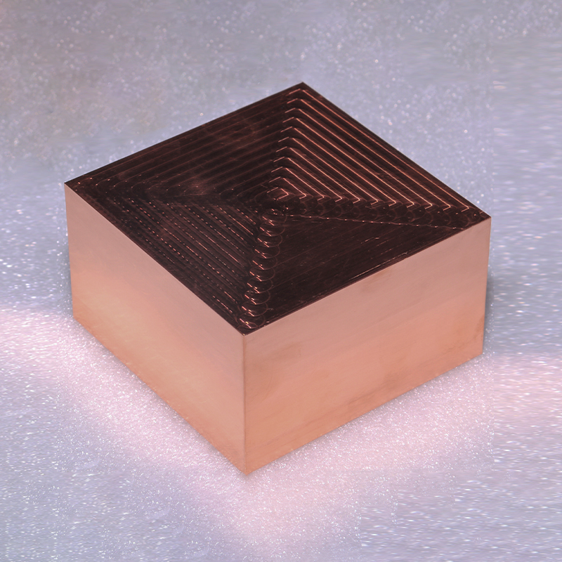
High purity copper (Cu) — available from 99.99% (4N) up to 99.99999% (7N) — is not interchangeable with standard industrial copper. In semiconductor interconnects, sputtering targets, and PVD evaporation processes, even a 0.001% impurity variance can cause film defects, resistivity spikes, or device failure. If you are sourcing copper for advanced manufacturing, purity grade is the single most critical specification.
What Purity Grades Actually Mean for High Purity Cu
The "N" notation used across the high purity materials industry describes the number of nines in the purity percentage. Each step up represents a tenfold reduction in total metallic impurities — a jump that has real consequences for electrical performance, film uniformity, and long-term device reliability.
| Grade | Purity (%) | Max Impurities (ppm) | Typical Application |
|---|---|---|---|
| 4N | 99.99 | 100 ppm | General electronics, busbars, heat sinks |
| 5N | 99.999 | 10 ppm | Semiconductor interconnects, LCD wiring |
| 6N | 99.9999 | 1 ppm | Advanced sputtering targets, PVD evaporation |
| 7N | 99.99999 | 0.1 ppm | Quantum computing, next-gen chip fabrication |
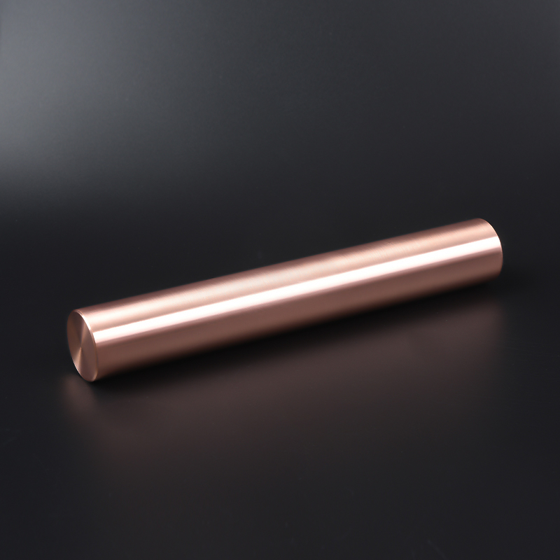
CRNMC supplies Cu ingots, targets, and evaporation materials reaching up to 99.99999% (7N) purity, with maximum ingot dimensions of 600 mm and weights up to 3 metric tons — figures that matter for high-volume production runs where consistency across large batches is non-negotiable.
The Role of High Purity Cu in Semiconductor Manufacturing
Copper replaced aluminum as the dominant interconnect metal in advanced logic chips starting in the late 1990s. The reason: Cu has approximately 40% lower resistivity than Al (1.68 vs. 2.65 micro-ohm-cm), which directly reduces RC delay — the time it takes signals to travel between transistors. As node sizes shrink below 5 nm, this advantage becomes even more decisive.
However, the performance gains only materialize when the copper used is genuinely semiconductor grade. Key concerns include:
- Alkali metals (Na, K): Concentrations above 0.1 ppm can cause threshold voltage shift in MOSFET devices by migrating through gate dielectrics.
- Transition metals (Fe, Ni, Cr): Deep-level traps in silicon that degrade minority carrier lifetime, reducing solar cell and DRAM performance.
- Oxygen content: High-quality Cu sputtering targets require oxygen levels below 1 ppm to prevent oxide inclusion in deposited films.
CRNMC's semiconductor-grade Cu products cover purity from 99.99% to 99.99999%, with packaging in export-standard wooden crates using double-layer vacuum sealing and pearl cotton cushioning — protecting against oxidation and mechanical damage from factory to fab.
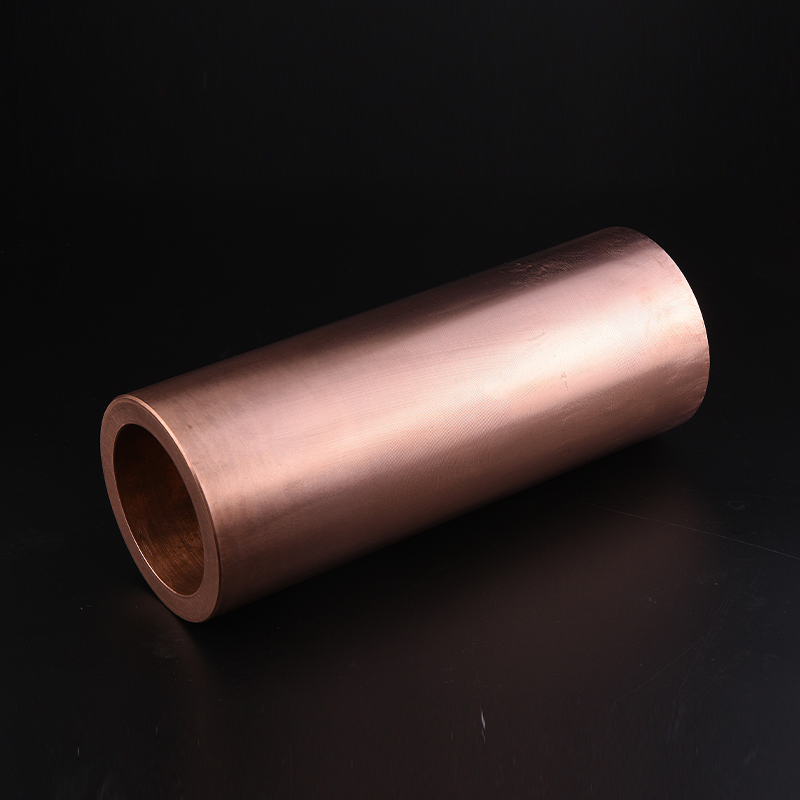
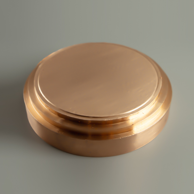
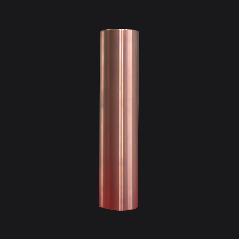
Cu Sputtering Targets: Specifications That Drive Thin Film Quality
Sputtering is the dominant PVD method for depositing copper thin films in semiconductor and flat panel display manufacturing. In a sputtering system, argon ions bombard the Cu target surface, ejecting atoms that travel to and coat the substrate. The quality of the deposited film is a direct function of target purity and microstructure.
Two microstructural properties determine target performance:
- Grain size: Fine, uniform grains (typically 50–150 micrometers) produce consistent sputtering rates and uniform film thickness across large substrate areas — critical for G8.5 generation LCD panels measuring over 2.2 x 2.5 meters.
- Density: Targets must reach near-theoretical density (above 99%) to minimize nodule formation — particulate defects that cause arcing and film pinholes.
CRNMC achieves these specifications through a multi-step process: high-purity Cu ingots are refined by multiple electrolysis and zone-refining passes, then formed by forging, rolling, and controlled heat treatment to refine grain structure before final precision machining. Targets are available in planar formats (up to 820 mm), rotatable configurations, and custom geometries including circular, rectangular, and annular forms.
Primary applications of Cu sputtering targets include:
- Semiconductor chip interconnect layers (logic and memory)
- Touch screen wiring and protective films
- Solar cell light-absorbing layers
- Flat panel display (FPD) electrode deposition
- Decorative and functional optical coatings
Cu Evaporation Materials: Pellets, Granules, and Process Compatibility
Evaporation materials are used in thermal evaporation and electron-beam (E-beam) PVD systems — processes that heat the source material until it vaporizes and condenses on the substrate as a thin film. For copper, the key physical parameters are a melting point of 1,083 degrees C and a vapor pressure of 10-4 Torr at 1,017 degrees C, which makes it well-suited for both thermal and E-beam processes.
High purity Cu evaporation materials are supplied in multiple forms to match different evaporation source configurations:
| Form | Typical Use Case | Purity Range |
|---|---|---|
| Pellets (2–6 mm) | Thermal boat evaporation, R&D systems | 99.99%–99.9999% |
| Granules | E-beam crucible loading, flexible fill | 99.99%–99.9999% |
| Slugs / Pieces | Large-area coating systems | 99.999%–99.9999% |
| Custom shapes | OEM evaporation source matching | Custom |
CRNMC packages Cu evaporation materials in double-layer vacuum sealed bags with inner PEF cushioning inside wooden crates — a configuration that maintains surface cleanliness and prevents atmospheric contamination before the material reaches the deposition chamber.
High Purity Cu in Superalloy and Aerospace Contexts
While semiconductor and display applications dominate demand for the highest purity grades, high purity Cu also plays a critical supporting role in superalloy manufacturing and aerospace components. Copper is a key alloying element in nickel-based superalloys used in turbine blades and combustion chambers, where trace impurity control during alloy preparation determines high-temperature fatigue resistance and oxidation behavior.
For these applications, 99.99% (4N) to 99.999% (5N) Cu stock is typically specified, with stringent controls on sulfur, bismuth, and lead — elements that embrittle grain boundaries at elevated temperatures. CRNMC's copper materials for aerospace and industrial applications are packaged in argon-purged galvanized drums with purity certifications traceable to batch-level ICP-MS analysis.
How to Specify High Purity Cu: A Practical Checklist
When placing an order for semiconductor grade Cu or high purity Cu for any advanced application, the following specification points should be confirmed with your supplier before committing to a purchase order:
- Purity grade and certification method: Confirm ICP-MS or GDMS analysis, not just GDOES, for trace-level impurity quantification below 1 ppm.
- Oxygen content specification: For sputtering targets, request oxygen below 1 ppm; for evaporation materials, below 5 ppm is generally acceptable.
- Form factor: Ingot, target blank, pellet, granule, tube, or custom machined part — confirm the supplier can process to final geometry.
- Dimensional tolerances: Critical for bonded targets and evaporation boats; confirm flatness, surface roughness (Ra), and parallelism requirements.
- Packaging and shelf life: Vacuum-sealed double-layer packaging is the minimum for 5N and above; confirm shelf life under storage conditions at your facility.
- Customs and export documentation: For international procurement, confirm HS code, country of origin certificate, and material safety data sheet availability.
Choosing a Reliable High Purity Cu Supplier
The difference between a reliable ultra high purity metals manufacturer and a commodity metals trader becomes clear in the details: batch-level traceability, consistent grain structure documentation, lead time for custom dimensions, and post-delivery technical support. CRNMC specializes in 5N to 7N copper products for semiconductor, LCD, solar, and aerospace customers, with customizable dimensions, certified analysis reports, and export packaging designed for global logistics. Whether the requirement is Cu sputtering targets for a new fab line, evaporation pellets for an optical coating system, or high-RRR copper for quantum computing components, the starting point is always the purity specification — and matching that specification to a supplier with documented process control.