English
Single Crystal: Structure, Growth Methods, and Industrial Applications
Content
Ask a metallurgist why a jet turbine blade is cast as a single crystal, and the answer comes down to one fact: grain boundaries are where materials fail first. At temperatures above 1,000 °C, those atomic-scale mismatches become nucleation sites for creep voids and cracks. Remove the grain boundaries entirely, and the same nickel-based alloy can operate roughly 100 °C hotter than its conventionally cast equivalent.
The same reasoning drives the semiconductor industry. A 300 mm silicon wafer must be sliced from a single-crystal ingot because any grain boundary beneath a transistor would scatter charge carriers and create electrical defects. Single crystals are not a niche laboratory curiosity; they are the structural foundation of modern electronics, aerospace propulsion, and precision optics. This article explains what a single crystal actually is, how conventional growth methods work, where single crystals deliver the most value, and what to check before you specify or purchase them.
What Is a Single Crystal?
A single crystal is a solid in which the crystal lattice is continuous and uninterrupted throughout the entire volume. The periodic arrangement of atoms repeats in three dimensions without a break, which is why a single crystal is sometimes described as one giant grain. There are no grain boundaries, no misoriented regions, and no structural discontinuities at the scale of the lattice.
That definition separates single crystals from the two other solid-state structures engineers usually choose between:
| Feature | Single crystal | Polycrystalline | Amorphous |
|---|---|---|---|
| Atomic arrangement | Continuous lattice | Many grains with random orientations | No long-range order |
| Grain boundaries | None | Present | Not applicable |
| Property variation | Anisotropic | Nearly isotropic | Isotropic |
| Typical examples | Silicon wafer, synthetic sapphire | Steel, cast aluminum | Glass, fused silica |
The practical consequence of this uniformity is predictability. In a single crystal, elastic modulus, electrical conductivity, and thermal expansion can be expressed as a function of crystallographic orientation. In a polycrystalline part, those properties are averaged over millions of randomly oriented grains, so the directional peak performance disappears.
Why Removing Grain Boundaries Improves Performance
The conclusion first: grain boundaries are the weakest link in a material's microstructure, and removing them improves high-temperature strength, electrical behavior, and optical transparency. Grain boundaries are high-energy regions with irregular atomic packing. Impurities tend to segregate there, dislocations pile up there, and cracks propagate along them. Three industries illustrate the practical effect.
Single-crystal turbine blades
In the hot section of a gas turbine, vanes and blades are made from nickel-based superalloys. The development path has moved from equiaxed casting to directionally solidified columns, and finally to single crystals. The improvement is measurable:
Typical maximum use temperature of nickel-based superalloy blades by casting route, in °C (approximate values).
That roughly 100 °C gain in temperature capability translates directly into higher turbine efficiency and lower fuel burn, which is why virtually every modern aero engine uses single-crystal blades in its first turbine stages.
Semiconductor wafers
In chip manufacturing, a silicon wafer is cut from a single-crystal ingot grown by the Czochralski method. Any grain boundary in the active area would act as a recombination center, causing leakage current and reducing yield.
Optical transparency
In optics, single-crystal sapphire is transparent from the ultraviolet through the mid-infrared and is mechanically strong enough for windows and domes. The polycrystalline form is translucent at best, because grain boundaries scatter light.
How Single Crystals Are Grown
All growth methods share one principle: they control solidification so that a single nucleus, or a seed crystal, dominates the process and no new grains form in front of the solidification front. Three methods cover most industrial production.
| Method | Typical materials | Advantage | Limitation |
|---|---|---|---|
| Czochralski | Silicon, sapphire, oxide crystals | Large ingots, mature process | Crucible contact can add impurities |
| Bridgman–Stockbarger | Nickel superalloys, compound semiconductors | Works for shaped parts, controlled gradient | Slower growth rates |
| Float-zone | High-purity silicon | Crucible-free, lowest contamination | Limited diameter, higher cost |
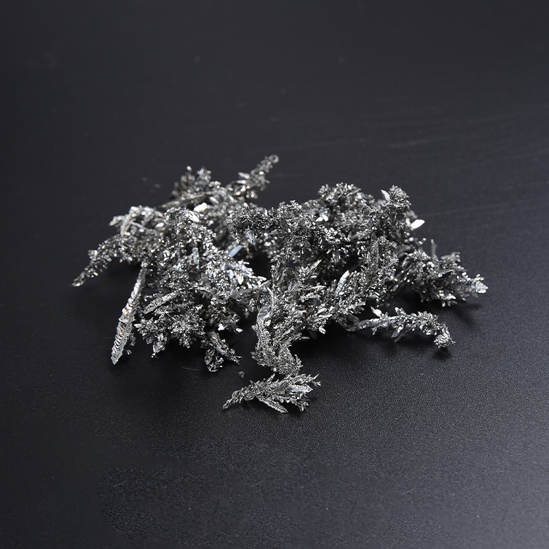
The starting material determines the upper limit of crystal quality. In Czochralski silicon growth, the feedstock is polycrystalline silicon refined to 99.9999999% purity. In Bridgman casting of superalloy blades, the master melt contains carefully refined nickel, cobalt, niobium, and other elements; any trace impurity in the charge ends up segregated at boundaries or trapped in the growing crystal. For researchers and smaller-scale producers working with titanium, a well-characterized starting material with a controlled crystalline morphology shortens process development. CRNMC supplies titanium crystals with documented purity, so customers do not have to rely on the lot-to-lot variation typical of commodity titanium sponge.
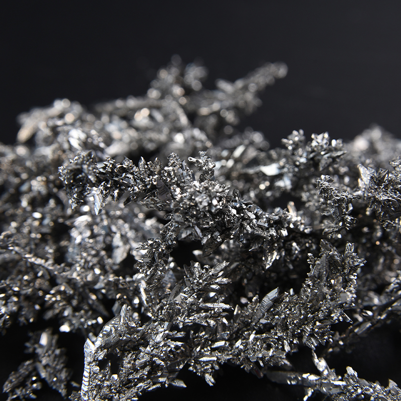 High-Purity Single-Crystal Titanium for Research and Advanced DepositionThis titanium crystal offers 99.98–99.99% purity with a controlled crystalline morphology, making it a reliable starting material for semiconductor sputtering targets and specialized research applications.View Product →
Industrial Applications of Single Crystals
Single crystals are used wherever property consistency, directional performance, or extreme purity is required. The approximate distribution of industrial demand is shown below; values are illustrative.
- Semiconductors 48%
- Aerospace 22%
- Optics 14%
- Other 16%
Illustrative distribution of single-crystal demand by end-use sector.
Semiconductor industry
Silicon wafers are the largest single-crystal product by volume. Beyond the wafer itself, the semiconductor supply chain depends on crystalline materials in other forms: sputtering targets for physical vapor deposition need a controlled grain structure and high purity to achieve uniform film thickness, and copper targets with a consistent grain size are widely used for interconnect metallization. These materials are manufactured to tight tolerances because a single defect in a target can disrupt an entire deposition run. The semiconductor materials segment of our site lists the relevant product forms and grades.
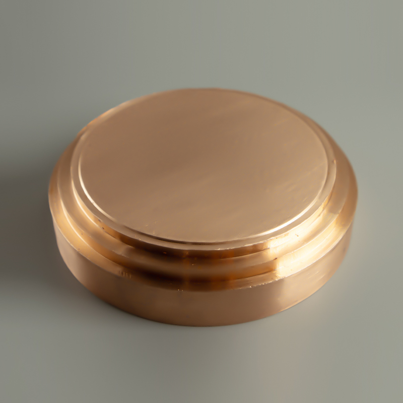 Ultra-High-Purity Copper Sputtering Target for Precision CoatingWith 99.999–99.9999% purity and customizable dimensions, this copper target ensures uniform film deposition in semiconductor and optical coating processes, reducing contamination and defects.View Product →
Aerospace and power generation
Single-crystal superalloy blades are the best-known aerospace application, but high-temperature alloys also rely on consistent refractory metal additions. Niobium, for example, forms stable strengthening phases and improves creep resistance in nickel-based superalloys. The same properties that make niobium critical in high-tech alloys also apply to superconducting magnets and aerospace components. Trace contamination in the niobium addition can destabilize the alloy's phase balance, so engine manufacturers specify tight impurity limits on every batch. For a more detailed review, our article on the properties of niobium explains why this metal appears in so many high-temperature designs.
 Large-Size High-Purity Niobium Ingot for Alloy and Semiconductor UseThis 99.99% pure niobium ingot, available up to 400 mm and 2 tons, supports consistent refractory metal additions in superalloys and serves as a key raw material for semiconductor-grade sputtering targets.View Product →
Optics and photonics
Sapphire, calcium fluoride, and YAG (yttrium aluminum garnet) single crystals are used in laser systems, infrared windows, and precision lenses because their uniformity keeps refractive index and absorption constant across the optical aperture.
What to Specify When Buying Crystalline Materials
Buyers who source single crystals or crystal-grade feedstocks usually evaluate four parameters: purity, orientation, structural integrity, and documentation.
- Purity grade. Purity is commonly expressed in nines: 99.99% (4N), 99.999% (5N), and 99.9999% (6N). The difference is not academic. At 6N levels, individual impurities are present at parts-per-million concentrations or lower, and each additional nine increases refining cost substantially.
- Crystallographic orientation. Because anisotropy is one reason to use a single crystal, the orientation must be defined for the intended property. A sapphire window for a pressure dome, for example, is often grown with the optical axis perpendicular to the window plane.
- Defect density. Dislocations, precipitates, and inclusions degrade electronic and mechanical performance. Characterization methods such as X-ray diffraction and preferential etching reveal the density of such defects.
- Traceability. A responsible supplier provides a certificate of analysis with a per-element impurity breakdown, not just a headline purity number.
The relationship between feedstock purity and downstream yield is direct. The chart below illustrates the typical effect of starting purity on the fraction of defect-free crystals in a growth campaign.
Illustrative relationship between feedstock purity and defect-free crystal yield. Actual results depend on material and process.
This is where a metal supplier's process depth matters. A company that performs purification, melting, casting, and machining in-house can control the entire chain from raw material to finished product, and can verify the result with purity testing. CRNMC applies this model to titanium, nickel, copper, niobium, and other specialty metals, which is why its products are used as feedstocks and crystalline products in demanding applications.
Frequently Asked Questions
What is the difference between a single crystal and a polycrystalline material?
A single crystal has a continuous, unbroken atomic lattice throughout its entire volume, with no grain boundaries. A polycrystalline material is composed of many small crystals, or grains, that meet at grain boundaries. The grain boundaries act as barriers to electron transport, sites for impurity segregation, and paths for crack propagation, which is why single crystals often outperform polycrystalline material when those properties matter.
Why are single crystals used in turbine blades?
Single-crystal blades eliminate grain boundaries that would otherwise weaken the alloy at high temperature. A single-crystal nickel-based blade can operate about 100 °C hotter than a conventionally cast blade, which improves engine efficiency and reduces fuel consumption.
How is purity measured in crystal-grade metals?
Purity is usually reported as a percentage such as 99.99% (4N) or 99.999% (5N), with the remainder consisting of trace elements. Glow discharge mass spectrometry (GDMS) and inductively coupled plasma mass spectrometry (ICP-MS) are common methods used to quantify each trace element. A certificate of analysis should list these values batch by batch.
Can any metal be produced as a single crystal?
In principle, most crystalline metals can be grown as single crystals, but the practical difficulty and cost vary enormously. Silicon, sapphire, and a few oxides are grown in industrial volumes. Nickel superalloys are cast as single-crystal components. Reactive metals such as titanium and niobium present more of a challenge because their melting points are high and their affinity for oxygen, nitrogen, and carbon requires specialized equipment.