English
High Purity Technology: Materials, Contamination Control, and Specifications
Content
- 1 High purity technology starts with the failure mode, not the label
- 2 What high purity means beyond the percentage
- 3 Where contamination enters and why metal supply deserves scrutiny
- 4 Material choices that make high purity practical
- 5 Verification: what a serious supplier should show
- 6 Specifying high purity technology without overpaying
- 7 FAQ: high purity technology in practice
- 8 A practical next step
High purity technology starts with the failure mode, not the label
High purity technology is the discipline of keeping unwanted atoms and particles out of a material, part, or gas stream, and proving that control lot after lot. It matters most where the process window is narrow: semiconductor fabrication, aerospace coatings, medical implants, flat-panel displays, and high-efficiency power devices. In those settings, one sub-micron particle or a few parts per million of an uncontrolled element can affect yield, adhesion, corrosion resistance, or electrical behavior.
A 4N or 5N label can look reassuring while still leaving a critical trace element or surface condition outside the specification. The practical question is not simply “what is the purity number?” but “which impurities affect my process, at what limit, and how is that limit verified?” That shift changes how buyers specify, sample, package, and audit high purity materials.
What high purity means beyond the percentage
Purity is usually a bundle of measurements. Bulk purity by difference may be expressed as 99.99% or 99.999%, yet the same lot can carry different levels of iron, oxygen, sulfur, sodium, or particles. For metals, gas elements and trace metals often matter more than the headline percentage. For targets and thin-film materials, grain structure and surface condition can matter as much as chemistry.
| Expression | Typical form | What it controls | What it can miss |
|---|---|---|---|
| Bulk purity | 4N, 5N, 6N | Total metallic impurity by difference | Individual trace elements and gas content |
| Trace element profile | ppb or ppm for Fe, Ni, Cr, Na, K | Process-specific contamination risk | Sampling location and surface cleanliness |
| Interstitial content | O, N, H, C in ppm | Mechanical, electrical, and melting behavior | Particles and handling contamination |
| Particle cleanliness | Counts per mL or per cm², maximum size | Defects in fabs, optics, and coatings | Dissolved metals and ionic residues |
| Surface and metrology | Roughness, oxide, grain size | Adhesion, bonding, corrosion, uniformity | Bulk chemistry and internal inclusions |
The useful specification links each number to a process risk. A titanium part for a medical device may need tight oxygen and iron control, while a copper target for display or semiconductor use may need low gas content, fine grain, and a clean surface.
Where contamination enters and why metal supply deserves scrutiny
High purity technology fails at the weakest handoff, not always at the melt. Contamination can enter through feedstock chemistry, scrap handling, crucible and refractory contact, furnace atmosphere, machining coolant, tool wear, cleaning rinses, gloves, packaging, and final installation. High-purity gas and piping systems show the same pattern: dead legs, permeation, outgassing seals, and improper purging can undo an otherwise clean supply chain.
- Feedstock and scrap can carry coatings, oil, or mixed-alloy residue that only appear in trace analysis.
- Melting and casting can introduce oxygen, nitrogen, carbon, or refractory particles.
- Machining can embed particles or leave coolant residues on apparently clean surfaces.
- Packaging and manual handling can add fibers, skin oils, and airborne particles after final testing.
For semiconductor applications, the qualification should cover the full route from incoming material to packed lot. Ask where the sample was taken, how the surface was prepared, and whether the test method can detect the element at the limit you actually need.
Material choices that make high purity practical
Metal selection should follow the failure mode. Titanium offers a strong strength-to-weight balance and corrosion resistance, but oxygen, nitrogen, iron, and surface condition can change ductility and downstream behavior. Titanium crystal and sponge routes are often used as starting stock for melting and alloy development.
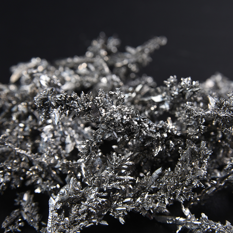 High-Purity Titanium Crystal for Semiconductor and AerospaceSingle-crystal titanium at 99.98–99.99% purity, relevant as starting stock and for sputtering targets where ordered structure and creep resistance matter.View Product →
Nickel is chosen for corrosion resistance, electronic components, and superalloy feed, where sulfur, phosphorus, oxygen, and trace metals need clear limits. A nickel ingot may be acceptable by bulk purity yet fail a downstream test if a specific trace element sits above the process window.
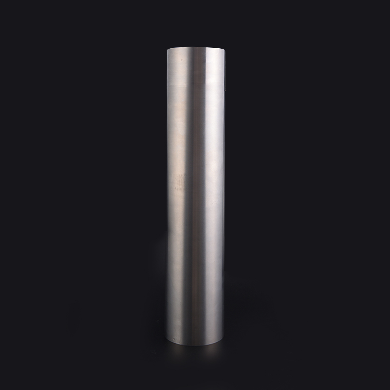 High-Purity Nickel Ingot for Semiconductor DepositionNickel ingot at 99.99–99.999% purity with controlled trace elements, intended for deposition targets, vacuum coating, and high-purity alloy smelting.View Product →
Copper is a conductivity material, but oxygen content, grain structure, and surface cleanliness influence sputtering, bonding, and joining. Copper targets and tubes therefore need chemistry and physical metrology considered together, not as separate purchasing checks.
 High-Purity Copper Sputtering Target for Thin FilmsCopper target at 99.999–99.9999% purity for PVD films, with customizable size and vacuum packaging to protect surface cleanliness.View Product →
Niobium and tantalum serve corrosion-resistant, high-temperature, and specialty applications; their interstitial content and inclusion control often decide performance. In practice, the best high purity technology choice is the grade that matches the smallest process window, supported by a supplier who can reproduce it across lots.
Verification: what a serious supplier should show
A certificate of analysis is a starting point, not the whole quality system. The supplier should be able to explain the analytical method, detection limit, sampling plan, lot traceability, cleaning route, and packaging control. At CRNMC, production covers purification, melting, casting, and machining across five sites, with ISO 9001 and IATF 16949 quality management, a purity testing entry point, and more than 60 registered technical patents. Those capabilities matter when they attach to a specific lot and specification rather than sitting in a brochure.
Ask how process changes are notified. A new crucible source, machining line, or cleaning agent can alter trace chemistry even when the drawing has not changed. Mature high purity purchasing treats change control as part of the product.
FAQ: high purity technology in practice
Does 5N purity mean a metal is ready for semiconductor use?
No. A semiconductor process may also care about specific trace metals, particles, surface oxide, outgassing, and documentation. The grade must be matched to the tool, process, and acceptance method.
Which is harder to control: trace metals or particles?
They are different problems. Trace metals usually begin with feedstock, melting, and refining. Particles often enter through machining, cleaning, packaging, and handling. Both need lot-level evidence.
Can high purity metals be machined without losing cleanliness?
Yes, with dedicated equipment, controlled coolant, tool-wear monitoring, validated cleaning, and final inspection. Machining is a contamination step and should be qualified as one.
What should a first quote include?
Application, material form, quantity, critical impurity list, test method, acceptance criteria, packaging, and delivery requirements. A supplier cannot quote responsibly against a purity label alone.
A practical next step
High purity technology works when chemistry, processing, packaging, and verification are designed as one chain. Start with the failure mode, set measurable limits, and ask for evidence at the lot level. If you are selecting ultra-high-purity metals for semiconductor, aerospace, biomedical, display, or new-energy applications, share your specification with our team and define the critical limits before the first lot is made.